

Keysight Launches Comprehensive Solution for Accurate and Seamless Photonic Circuit Design

Keysight Launches Comprehensive Solution for Accurate and Seamless Photonic Circuit Design
- Optimizes photonic integrated circuit performance with advanced physics-based simulation
- Eliminates fragmented workflows and improves design accuracy with a holistic photonic design automation tool
- Ensures compliance and manufacturing readiness with process design kit customization and real-world data integration
SANTA ROSA, Calif.--(BUSINESS WIRE)-- Keysight Technologies, Inc. (NYSE: KEYS) announces the launch of Photonic Designer, an innovative photonic design automation (PDA) software solution engineered to provide unparalleled accuracy and compliance-driven design validation. Designed for photonics design engineers, this solution enables streamlined workflows from concept to simulation, emulation, and manufacturing, addressing the challenges of fragmented tools, inconsistent simulation precision, and increasing compliance demands.
This press release features multimedia. View the full release here: https://www.businesswire.com/news/home/20250319611958/en/
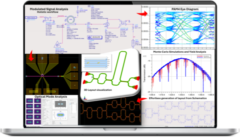
From concept to validation—Photonic Designer streamlines the entire photonic design process with a comprehensive automation solution.
Photonics design engineers often face challenges with scattered tool chains and simulation discrepancies that hinder efficiency and precision. Traditional workflows require engineers to switch between multiple software platforms, making it challenging to ensure design consistency. Keysight’s Photonic Designer, part of the Advanced Design System (ADS) suite of tools, eliminates these inefficiencies by offering a comprehensive, physics-driven simulation environment that accurately predicts real-world circuit performance. Keysight tools also support an open, interoperable workflow ecosystem for maximum flexibility.
Photonic Designer integrates real-world measurement data directly into the simulation workflow, to optimize models and streamline compliance and validation. This allows engineers to:
- Verify designs against industry modulation standards before fabrication.
- Use models with best-in-class simulators to ensure accurate, confident, robust designs.
- Ensure seamless compatibility with foundry PDKs to avoid costly iterations.
- Optimize photonic model variables to match foundry processes to align with manufacturing conditions.
- Automate and accelerate design verification, reducing go-to-market time.
The software is designed to streamline pure optical and combined electrical-optical-electrical workflows for circuit design, providing an intuitive interface for effortless circuit design and layout generation. Engineers can simulate, validate, and optimize photonic circuits while ensuring compliance with stringent design rules, guaranteeing precision and reliability.
To further enhance the design process, CompoundTek, a leading provider of photonics foundry services, is offering a Photonic Designer PDK for Keysight ADS users, for their silicon photonics process. This collaboration enables engineers to develop PICs with foundry-verified components, ensuring seamless transition from design to fabrication.
S. Gunasagar, Chief Operating Officer at CompoundTek said: “We are excited to offer a highly accurate PDK for our silicon photonics process. This integration with Keysight’s ADS allows engineers to confidently design and validate photonic circuits with the assurance of manufacturing compatibility, ultimately accelerating time-to-market for innovative solutions.”
Nilesh Kamdar, EDA Design & Verification General Manager at Keysight, said: “Engineers need a reliable and precise environment to design and validate photonic integrated circuits without unnecessary tool-switching. Photonic Designer provides a single, unified platform that integrates physics-based simulations, PDK customization, and compliance verification, ensuring high-fidelity results from concept to manufacturing.”
Resources
- Application Note: Optimizing Photodetector Model to a Silicon Photonics Foundry Process
- Product Page: Photonic Designer
- Video: Photonic Designer
- Video: How to use the Optical Mode Solver from Keysight Photonic Designer
More Information: Attend the Keysight Booth at OFC 2025
Visit the Keysight booth #1301 at the OFC 2025 conference to learn more about Photonic Designer and its capabilities.
About Keysight Technologies
At Keysight (NYSE: KEYS), we inspire and empower innovators to bring world-changing technologies to life. As an S&P 500 company, we’re delivering market-leading design, emulation, and test solutions to help engineers develop and deploy faster, with less risk, throughout the entire product life cycle. We’re a global innovation partner enabling customers in communications, industrial automation, aerospace and defense, automotive, semiconductor, and general electronics markets to accelerate innovation to connect and secure the world. Learn more at Keysight Newsroom and www.keysight.com.
View source version on businesswire.com: https://www.businesswire.com/news/home/20250319611958/en/
Contacts
Keysight Media Contacts
North America PR Team
pdl-americas-keysight@keysight.com
Fusako Dohi
Asia
+81 42 660-2162
fusako_dohi@keysight.com
Jenny Gallacher
Europe
+44 118 927 4003
jenny.gallacher@keysight.com
Source: Keysight Technologies, Inc.
Smart Multimedia Gallery
From concept to validation—Photonic Designer streamlines the entire photonic design process with a comprehensive automation solution.


View this news release and multimedia online at:
http://www.businesswire.com/news/home/20250319611958/en